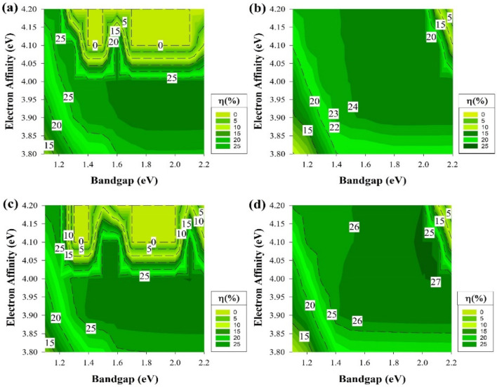
Figure 12.
The efficiency of four proposed structures, including a-Si:H passivating layers as a function of Eg and χ for doped layers with defects at the 0.2 eV level below Ec. (a) Contour graphs of the n-i-p structure with p-type wafer base. (b) Contour graphs of the n-i-p structure with n-type wafer base. (c) Contour graphs of the p-i-n structure with the p-type wafer. (d) Contour graphs of the p-i-n structure with n-type wafer base.

