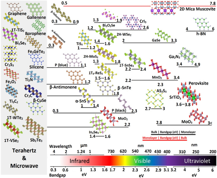
Fig. 1.
2D materials are chosen for their experimental significance and demonstration, with depictions of a perspective view of their crystal structures. The arrangement is following their bandgap, guided by the bottom wavelength/bandgap scale, whereas the bar beneath each structure indicates the bandgap range from bulk to monolayer. Typically, the bulk bandgap is smaller than that of its monolayer (black bars), but there are exceptions (red bars). 2D materials on the far left, indicated by a gray box, are zero or near-zero bandgap, metallic, or semimetallic [8]

