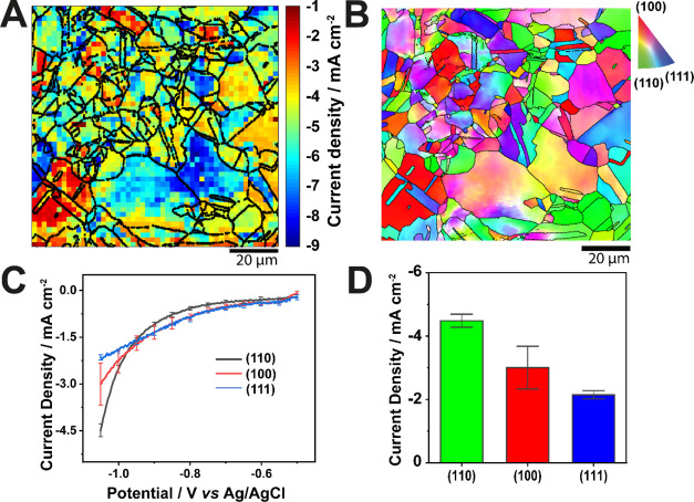
Figure 2.
(A) Electrochemical image of a polycrystalline Cu surface, extracted from the potentiodynamic SECCM movie (Supporting Information, Movie S1) at Esurf = −1.05 V vs Ag/AgCl with overlay of grain boundaries (black solid lines) from (B) co-located EBSD map. The scan covers a 100 by 100 μm2 area composed of 2500 pixels. SECCM mapping was conducted with a nanopipette filled with 10 mM KHCO3 in a CO2-purged environmental cell. (C) Average linear sweep voltammograms obtained on grains closest to the low-index crystallographic orientations presented in blue, red, and black for (111), (100), and (110) respectively. ±1 standard deviation bars for the linear sweep voltammograms are provided at 50 mV intervals. (D) Bar chart and the current density at −1.05 V vs Ag/AgCl for the low-index grains in the electrochemical map (A), with N = 7, 17, and 24 for (111), (100), and (110) respectively.

