Figure 1.
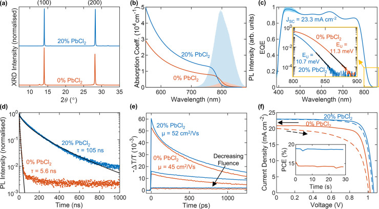
PbCl2 substitution improves device performance. (a) X-ray diffraction (XRD) patterns of FA1–yCsyPb(I1–xClx)3 full photovoltaic devices after testing, grown with (blue line) and without (red line) PbI2 substituted for PbCl2, as denoted in the figure. The XRD patterns were acquired with a Cu–Kα 1.54 Å X-ray source, corrected for specimen displacement, and normalized. (b) Absorption coefficient of bare thin films of the aforementioned composition on z-cut quartz. The shaded region shows the unnormalized PL after photoexcitation at 470 nm. (c) External quantum efficiency (EQE) of a device with 20% PbCl2 and the corresponding integrated short-circuit current (JSC). The inset shows the absorption edge from the EQE and the Urbach tail fit (black line). (d) Time-resolved photoluminescence (PL) traces for thin films of the aforementioned bare films on quartz, after photoexcitation by a 1 MHz pulsed 470 nm laser at a fluence of 20 μJ/cm2. The black line shows a stretched exponential fit. (e) Optical-pump THz-probe (OPTP) photoconductivity transients of the aforementioned bare films on quartz after photoexcitation at 400 nm as a function of fluence (1.0, 10, 42 μJ/cm2). (f) Current–voltage (J–V) measurements of the aforementioned photovoltaic devices under AM1.5 illumination, as measured under reverse bias (solid line) and forward bias (dashed line). The inset shows the power conversion efficiency (PCE) measured at the max power point under continuous illumination over 30 s.

