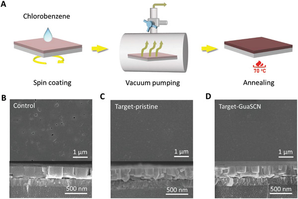
Figure 1.

Formation of 2D/3D vertical heterojunction in the perovskite film via vacuum treatment. A) Schematic diagram of the vacuum assisted fabrication process of Sn‐based perovskite thin film. B) SEM images of the perovskite film prepared through the conventional spin coating method without vacuum treatment. C) SEM images of the perovskite film prepared with vacuum treatment. D) SEM images of the vacuum treated perovskite film containing 2.5% GuaSCN. Specifically, the cross section SEM images corresponding to each sample are shown on the bottom in (B–D).
