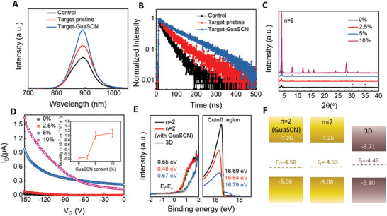
Figure 3.

Charge dynamics and electrical characterizations of perovskite films. A) PL spectra of the Sn‐based perovskite films. B) TRPL spectra of the Sn‐based perovskite films. C) XRD patterns of the quasi‐2D PEA2FA1Sn2I7 perovskite films processed with different amounts of GuaSCN. D) Transfer curves of the field‐effect transistors prepared by depositing PEA2FA1Sn2I7 perovskite films (containing different amounts of GuaSCN) on SiO2/Si substrates. Inset: the calculated hole mobility of the corresponding films. E) UPS spectra of the 3D FASnI3 and PEA2FA1Sn2I7 (w/o or w/10% GuaSCN) perovskite films. F) Energy level diagram of the quasi‐2D perovskite PEA2FA1Sn2I7 (w/o or w/10% GuaSCN) and 3D FASnI3 films.
