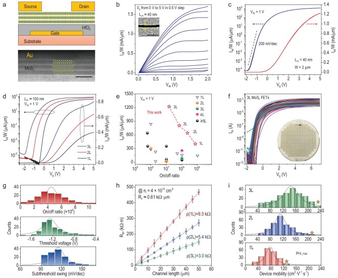
Figure 4.
Benchmark testing of multi-layer MoS2 FETs. (a) Schematic view (top) of back-gated MoS2 FET and cross-section STEM image (bottom) of a trilayer FET at the MoS2–Au contact region. Scale bar: 1 nm. (b and c) Typical output/transfer curves of a trilayer MoS2 FET. Lch = 40 nm, tHfO2 = 5 nm. Inset to (b) shows the SEM image of the channel. Scale bar: 200 nm. (d) Comparison of transfer curves of mono-, bi- and trilayer MoS2 FETs with Lch ≈ 100 nm. (e) The comparisons of current densities (@Vds = 1 V) and on/off ratios with previous works. The detailed device parameters are shown in Supplementary Table S1. (f) Transfer curves of 150 trilayer MoS2 FETs at Vds = 1 V. Lch = 5–50 μm, tHfO2 = 10 nm. Inset to (f) shows photograph of wafer-scale MoS2 FET array. (g) Statistical distribution of on/off ratio (red), threshold voltage (green) and subthreshold swing (blue) from the 150 trilayer MoS2 FETs. (h) The sheet resistance ρ and contact resistance Rc extracted from mono-, bi- and trilayer MoS2 FETs. (i) Statistical distribution of device mobility of mono-, bi- and trilayer MoS2 FETs. The yellow stars indicate the maximum values achieved in each type of device.

