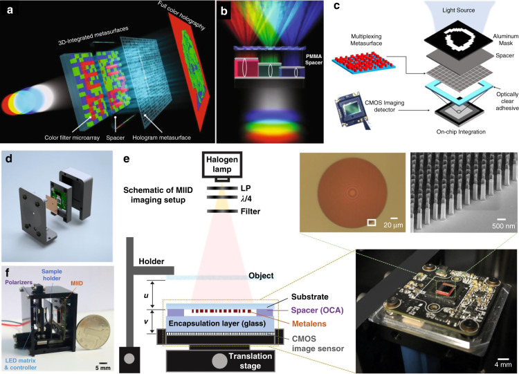
Fig. 19. Integration of metasurface and photosensor wafers using stacking and packaging technologies.
a Exploded view of 3D-integrated metasurfaces for full-color holography. b Front view of three micro-units of the 3D-integrated metasurfaces. PMMA is used as a spacer. c Exploded schematic diagram of the stacked metasurface integrated with a CMOS chip. d Setup of the 3D-printed system integrating the metalens with a photosensor. e Schematic of the optical setup for the metalens-integrated imaging device. Zoomed out are the photograph (down), top-view optical microscope image (top left), and side-view SEM image (top right) of the fabricated metalens. f Photograph of the prototype. Panels a and b are reproduced with permission215. Copyright 2019, The Authors, published by Springer Nature. Panel c is reproduced with permission216. Copyright 2022, The Authors, published by Springer Nature. Panel d is reproduced with permission63. Copyright 2020, American Chemical Society. Panels e and f are reproduced with permission60. Copyright 2020, The Authors. Published by SPIE

