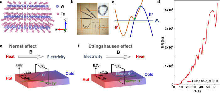
Fig. 1. WTe2 basic properties and the Nernst–Ettingshausen effect.
a Crystal structure of WTe2. Te–Te layers in the ab-plane are bonded by van der Waals forces and the crystals can be cleaved easily. b Photograph of WTe2 single crystals, and the spelling of “WTe2” using artificially deformed crystals. Inset shows a Möbius strip formed from a WTe2 single crystal. c Schematic of the band structure of WTe2 Weyl semimetal. Electrons and holes show nearly perfect compensation at the Fermi energy. The green dots show a pair of Weyl points, which are above the Fermi energy. d Magnetoresistance of the studied WTe2 single crystal at 0.85 K recorded using a magnetic-field pulse up to 65 T. e Schematic illustrations of Nernst effect. f Ettingshausen effect. The orientation of the experimental setup corresponding to the crystal axes is shown. Both the Nernst and Ettingshausen devices need only one material, and therefore have lower complexity than Seebeck devices.

