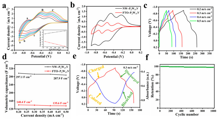
Figure 5.
(a) CV for the NW−P2W17V film at different scan rates (from inner to outer): 50, 70, 90, 110, 130, and 150 mV s−1. The inset shows plots of the anodic and the cathodic peak currents for C-c against scan rates; (b) CV for NW−P2W17V and FTO−P2W17V films at a scan rate of 50 mV/s; (c) Charge/discharge curves of NW−P2W17V film at various current densities; (d) Volumetric capacitance at various current densities of NW−P2W17V and FTO−P2W17V films; (e) In situ transmittance evolution at 580 nm with the charging and discharging process of the NW−P2W17V film; (f) Cycle performance of NW−P2W17V film measured under a current density of 0.2 mA cm−2.

