Figure 5.
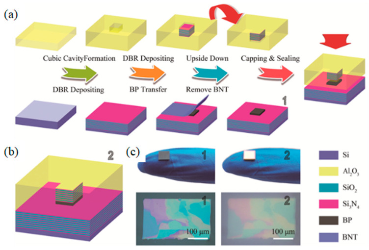
(a) Manufacturing process of BP laser is designed with an open cavity surface emitting laser device. Using sapphire as the substrate, DBR is deposited in the cubic step hole, bonding the substrate reverse. After preparing the steps for DBR deposition on the silicon substrate and bottom assembly, transfer the Nitto tape with blue Nitto tape, and finally combine them to obtain the laser device. (b) Schematic diagram of the completed laser device. (c) The image on the left shows the BP film covering the waveguide and the optical micrograph, while the image on the right shows the final image and the optical micrograph of the device [211]. Copyright 2019 American Chemical Society.

