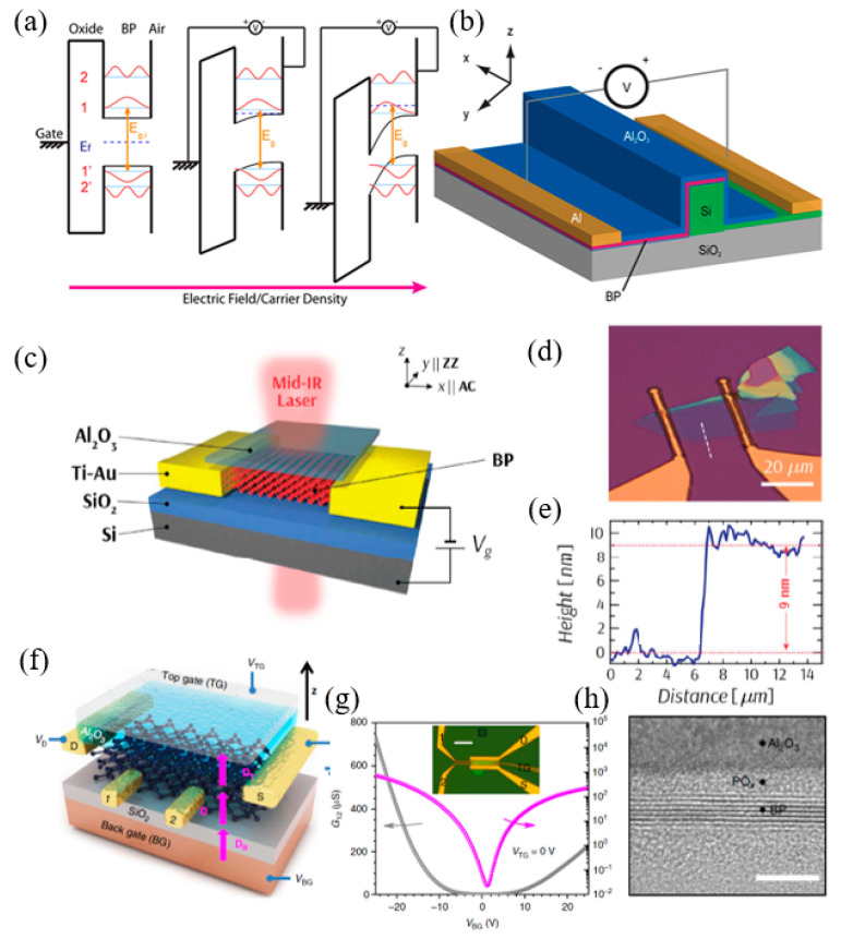
Figure 13.
(a) Schematic diagram, band diagram, and wave function of 5 nm thick BP QW. (b) Modulator schematic [276]. (c) Schematic diagram of multilayer BP modulator. (d) Optical microscope image of BP modulator. (e) Atomic force microscope image of BP modulator [277]. Copyright 2017 American Chemical Society. (f) Test program for BP band gap tuning. (g) 4 nm thick BP film conductance as a function of top gate zero bias voltage and back gate bias voltage. (h) BP under an atomic microscope [278]. Copyright 2017 Nature Publishing Group.

