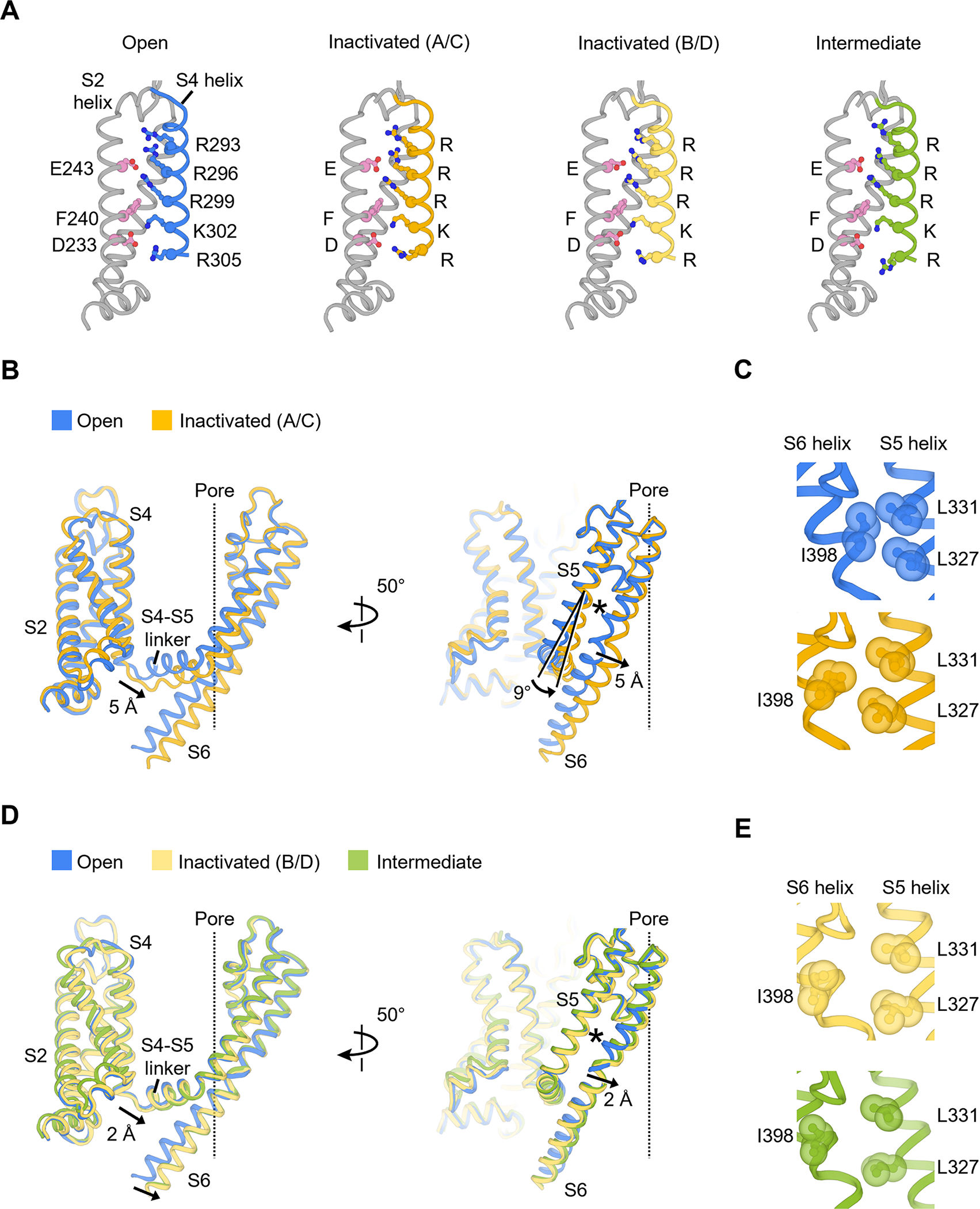
Figure 3. Conformational changes of KV4 during closed-state inactivation.

(A) Structures of voltage sensor during inactivation. Residues composing the gating charge transfer center (E243, F240 and D233) and positively charged residues on the S4 helix are shown as ball-and-stick representation.
(B) Conformational changes of the S4-S5 linker and S5-S6 helices in the inactivated state (chain A/C). The central ion pathway is represented by a dash line. The asterisk symbol highlights the location of the interaction shown in (C).
(C) Hydrophobic patch between S5 and S6 helices that controls the upper gate I398 (open state, blue; inactivated state, yellow).
(D) Conformational changes of the S4-S5 linker and S5-S6 helices in the inactivated state (chain B/D) and intermediate state. The central ion pathway is represented by a dash line. The asterisk symbol highlights the location of the interaction shown I).
(E) Hydrophobic patch in the inactivated state (chain B/D, light yellow) and intermediate state (green).
