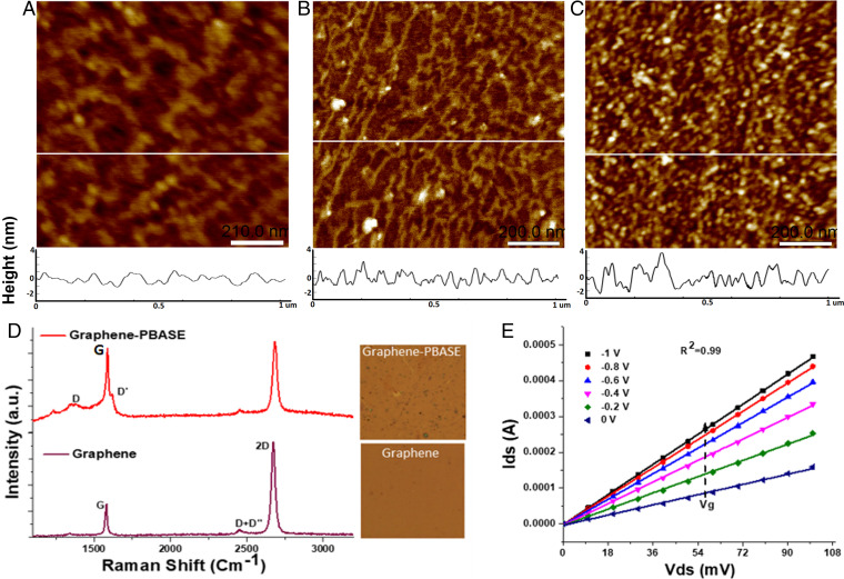
Fig. 2.
GFET characterization—atomic force microscopy height mode images of GFET surface after different steps: (A) bare graphene surface, (B) after 5 mM PBASE addition, and (C) after 1 μM aptamer functionalization. (Scale bars, 200 nm; z scale in all images, 0 to 7.5 nm.) The white horizontal line in each image represents a section through the image whose height profiles (in nanometers) are included below each respective image. (D) Raman spectroscopy of pristine graphene and PBASE-functionalized GFET (Inset shows light microscope image of scanned area). (E) Transfer characteristics (IDS vs. VDS) of GFET derivatized using PBASE (5 mM) were analyzed by sweeping VGS from 0 to −1 V at 0.2V steps and variable drain source voltage (VDS) of 0 to 100 mV with incremental steps of 10 mV.

