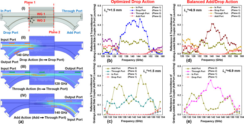
Fig. 4. Numerical study of the grating-loaded side couplers.
a (I) 3D model of the ADM circuit used in simulations that comprises two Y-splitters and a 35-mm-long grating-loaded side coupler (20 grating periods with Λ = 1.03 mm, H = 0.21 mm). The computed electric field distributions in the ADM circuits for various launching conditions: (II) In port at 140 GHz (grating stopband), (III) In port at 128 GHz (grating passband), and (IV) Add port at 140 GHz (grating stopband). Optimized Drop Action: reflectance and transmittance of various ports under b In port launching and c Add port launching. Balanced Add/Drop Action: reflectance and transmittance of various ports under d In port launching and e Add port launching. Panels b–e are computed using Eq. (1) and data from (a).

