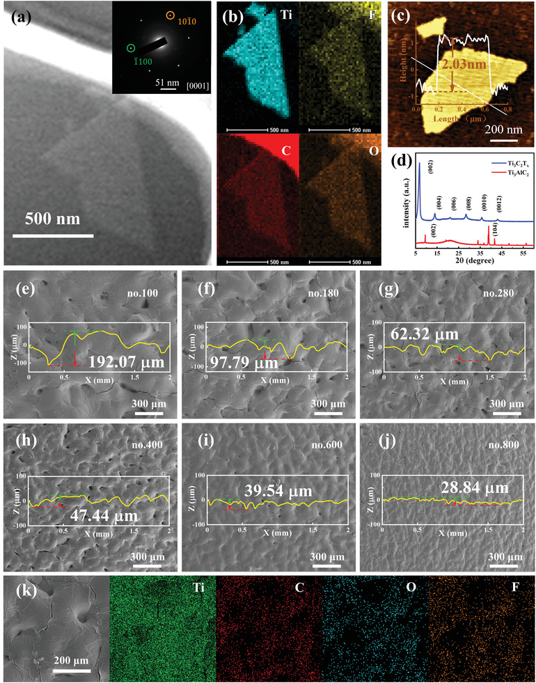
Figure 2.

a) TEM image of the MXene nanosheets, and the inset is the corresponding SAED pattern. b) energy dispersive spectrometer (EDS) mapping images of MXene (Ti3C2T x ). c) AFM image of the MXene nanosheet. d) XRD pattern of the MAX phase (Ti3AlC2) and MXene Ti3C2T x nanosheet. e–j) SEM images of the sensitive layers with the different spinosum structures (nos.100, 180, 280, 400, 600, and 800). k) EDX mapping images of no. 280 sensitive layer.
