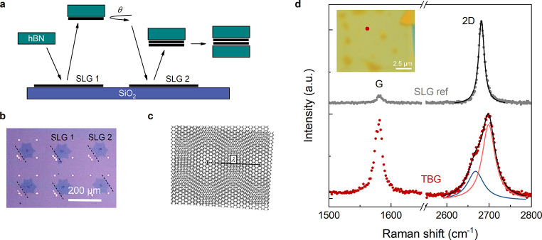
Figure 1.
(a) Schematics of the dry pick-up process with stacking of separated CVD-grown graphene crystals. (b) Optical microscopy image of CVD SLG crystals on SiO2/Si. The dashed lines indicate their crystallographic alignment. (c) The θ-rotated graphene sheets form a moiré pattern with periodicity λ. (d) Representative Raman spectrum of TBG (dark red), compared to a SLG reference (gray). The light red and blue lines are the two Lorentzian components of the TBG 2D peak. Inset: optical microscopy image of hBN-encapsulated SA-TBG. The dark red spot indicates the point where the TBG spectrum in the main panel is acquired.

