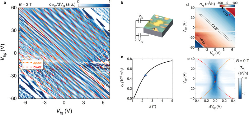
Figure 2.
(a) First derivative of the Hall conductivity as a function of top and back-gate voltages, measured for a fixed value of the applied perpendicular magnetic field (B = 3 T). The dotted orange (red) lines are the calculated positions of Landau levels from the upper (lower) graphene layers, employing vF = 0.47 × 10⁶ m/s and Cgg = 17.5 × 10⁻⁶ F/cm2. (b) Schematics of the gating configuration. The optical microscopy image of the device is taken before the final etching step; the scale bar is 2.5 μm. (c) Fermi velocity of TBG as a function of the twist angle, calculated according to the theory described in refs (54 and 55) and references therein. Results in this figure have been obtained by setting u0 = 79.7 meV and u1 = 97.5 meV, where u0 and u1 are the intra- and intersublattice interlayer tunneling amplitudes, respectively. The blue circle corresponds to the vF value estimated for our device. (d) Hall conductivity as a function of the gate voltages (same gate ranges and magnetic field as in (a)). The sign changes in σxy correspond to the sample CNP and the two vHs. The black rectangle indicates the gate range considered in panel (e), the black and dark red dots are the gate values used for the measurements in Figure 4. (e) Zero-field longitudinal conductivity (lg scale) as a function of top-gate voltage relative to the sample CNP and back-gate voltage. The dotted orange (red) line is the calculated charge neutrality point for the upper (lower) layer. All the data in this figure have been acquired at T = 4.2 K.

