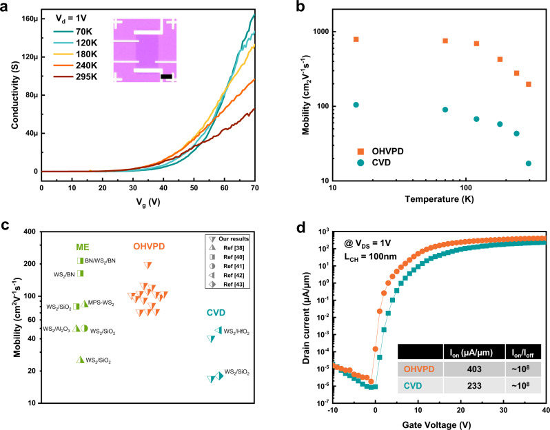
Fig. 4. Electrical performance of OHVPD-WS2 monolayers.
a Four-probe conductivity as a function of Vg for OHVPD-WS2 monolayer device on the 300 nm SiOx substrate at different temperatures. Insect shows the device structure. (Scale bar: 5 μm) b Field-effect mobility as a function of temperature for OHVPD- and CVD-WS2 monolayers. c Comparison of mobility distribution for our OHVPD-WS2 results (orange), mechanical exfoliation WS2 monolayers (ME, green), and conventional CVD-WS2 (cyan) from literatures. d FET transfer curve of an OHVPD-WS2 monolayer for the short channel device (LCH = 100 nm).

