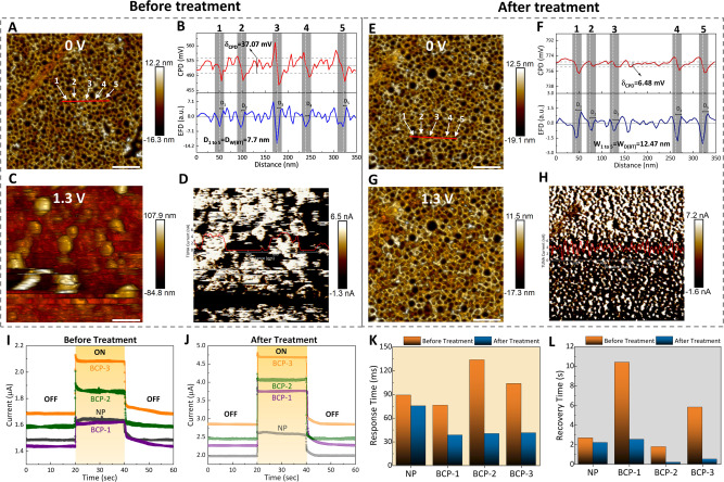
Figure 6.
Atomic force microscopy (AFM) and photoelectrochemical response of samples before and after plasma treatment. Topography at applied bias voltages of A, E) 0 V and C, G) 1.3 V with D, H) equivalent current profile by PeakForce tunneling atomic force microscopy (PF‐TUNA), scale bar=200 nm. Contact potential difference (CPD) and its derivative, electrical field difference (EFD) observed from a red line of 350 nm across 5 indicated pores B) before and F) after plasma treatment. Photoelectrochemical response on samples I) before and J) after plasma treatment, with respective K) response and L) recovery time for CuTe film.

