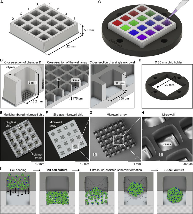
Figure 1.
Design of the microwell chip platform
(A) Illustration of the multichambered microwell chip, including numbers and letters to indicate the columns and rows of the 4 × 4 chambers.
(B) Cross-section illustrations of the chip with notations of dimensions and materials. Left: a single chamber (position D1) with a microwell array at the bottom is shown. Middle: a microwell array is shown. Right: a single microwell is shown.
(C) Illustration showing the chip placed in a Ø 35-mm-round chip holder (the colored chambers illustrate the use of different experimental liquid conditions in each chamber). The chambers are accessible for pipetting from above, and imaging is done from below by an inverted microscope.
(D) Illustration of the chip holder alone, with its 22-mm-wide slot for the chip visible in the middle of the holder.
(E and F) Photographs of the multichambered microwell chip (E) and of the Si-glass microwell chip without a bonded polymer frame (F).
(G and H) Scanning electron micrographs of a 6 × 6 microwell array in the bottom of a chamber on the chip (G) and of a single 350 μm microwell (H).
(I) Illustrations with a top-perspective view of the formation of 2D and 3D cell cultures in a microwell. From left to right: seeding of cells into a microwell, a 2D monolayer cell culture, formation of a cell aggregate using USW in the microwell, and the resulting 3D spheroid cell culture are shown.

