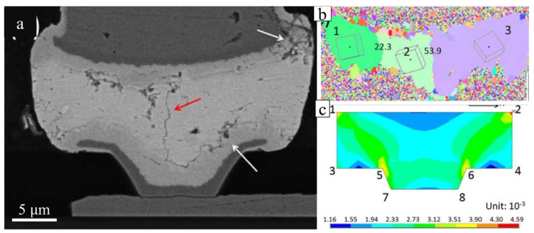
Figure 13.
(a) SEM image of a microbump with crack propagation (pointed out by the red arrow) along the grain boundary with high misorientation (53.9°) near the corner with high thermal strain after the TCT. (b) EBSD orientation map (the boxes show the Sn crystal unit cells in the solders, and the numbers are the misorientations of the boundaries) and (c) thermal strain distribution shown via finite-element method simulation in the microbump of (a). Reprinted with permission from ref. [102]. Copyright 2017 Springer Nature.

