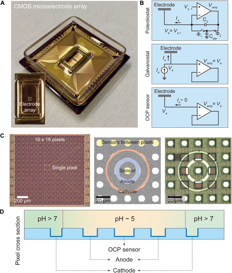
Fig. 1. CMOS electrochemical cell array.
(A) Image of the packaged CMOS IC featuring a predefined array of 64 × 64 = 4096 Al pads. (B) The CMOS circuit connected to each Al pad can be configured into one of the three modes: potentiostat, galvanostat, and OCP sensor. (C) Pt electrodes are postfabricated on top of the predefined Al pad array, resulting in an array of 16 × 16 = 256 electrochemical cells or pixels. Each pixel consists of an inner anodic Pt ring electrode connected to a set of four underlying Al pads, an outer cathodic Pt ring electrode connected to another set of four underlying Al pads, and a center OCP sensor with a circular Pt electrode connected to one underlying Al pad. In addition, circular Pt electrodes (with each connected to one underlying Al pad) are postfabricated in between pixels to be used as additional OCP sensors. A scanning electron microscope image and an optical image of a pixel and its surrounding are shown in the middle and at the right, respectively. (D) In any given pixel, if both of its two concentric rings are operated in the galvanostat mode with the outer cathodic ring with a negative current injection and the inner anodic ring with a positive current injection, the base generated by the former serves as an electrochemical wall that confines the protons electrochemically generated by the latter.

