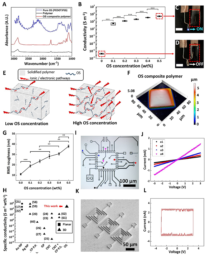
Figure 3.

Chemical, electrical, and physical characterization of MPL-fabricated microstructures. A) FTIR spectra of pure OS (blue curve), OS composite polymer (red curve) and polymer (black curve) microstructures. B) Electrical conductivity of OSCMs with respect to OS concentration in the resin. Data shown as mean ± SD, n = 9, *** p<0.001. In the box graph, black squares, horizontal lines and box range demonstrate mean, median, and SD, respectively. C and D) OS composite polymer structures (C) and polymer structures (D) acting as interconnects to drive a LED, respectively (scale bars: 5 mm). E) Schematic of proposed conductivity of MPL-fabricated OS composite polymers. F) 3D view of color-coded height maps of cubic microstructures fabricated using OS composite resin (0.5 wt% OS), showing surface texture of MPL-fabricated microcubes. G) Surface roughness (Rrms) with respect to OS concentration. Data shown as mean ± SEM, n = 4, ** p<0.05, *** p<0.001. H) Comparison between specific conductivity of MPL-fabricated conductive microstructures in this study using OS composite resin and prior works using other conductive nanomaterials and post processing methods (Au NP: gold nanoparticles, Ag NP: silver nanoparticles, CP P.P.: conducting polymer (CP) post-polymerization (P. P.) after MPL fabrication, GP: Graphene, CNT: carbon nanotubes, CNT + CP P.S. : Doping CNT in resin, followed by post soaking of MPL-fabricated structures in CP solution, OS: organic semiconductor). Black squares represent planar structures, black triangles represent 3D microstructures. I) Optical microscopy micrograph of a μPCB comprised of various electrical elements. J) I-V graph of elements in μPCB: a1 (black squares), a2 (red circles), a3 (blue up-sided triangles), and a4 (magenta down-sided triangles); the straight lines indicate the resistor behavior of the elements. K) SEM micrograph of a microcapacitor array. L) Hysteresis loop of three microcapacitors in parallel. The rectangular-shaped I-V indicates capacitor behavior.
