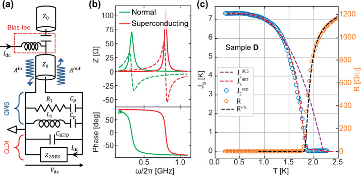
Fig. 4. Microwave measurement of the KTaO3 2-DEG.
a Schematics of the measurement setup adapted from ref. 26. The contribution of the sample is represented by the 2-DEG impedance, Z2DEG, and the parallel capacitive contribution of the KTaO3 substrate, CKTO. SMD components, resistor R1 = 75 Ω, inductor L1 = 6.5 nH, are placed in parallel to define a resonating circuit. Large SMD capacitors Cp = 2μF block the dc signals in L1 and R1 without influencing the signals at microwave frequencies. The reflection coefficient at the circuit sample Γ(ω) = is extracted from the measurement as described in ref. 26. A bias-tee is used to separate the dc current and the microwave one. b Top: Real (full lines) and imaginary (dashed lines) parts of the 2-DEG impedance as a function of frequency in the normal state at T = 2.5 K and in the superconducting state at T = 0.2 K after a calibration procedure26. Bottom: corresponding phases of the 2-DEG impedance in the normal and superconducting state. The resonance frequency of the sample circuit can be clearly identified, for instance, as the maximum of the peak in the real part of the impedance or as a π phase shift in its phase. c Superfluid stiffness extracted from the resonance frequency and Eq. (1) as a function of the temperature. The dashed purple line shows an attempt to fit the experimental data within a standard BCS model (), which provides a mean field = 2.3 K. A better agreement is obtained by using a BKT model (). On the right axis, the figure also shows the sheet resistance curve (R) fitted with the Halperin and Nelson formula (RHN).

