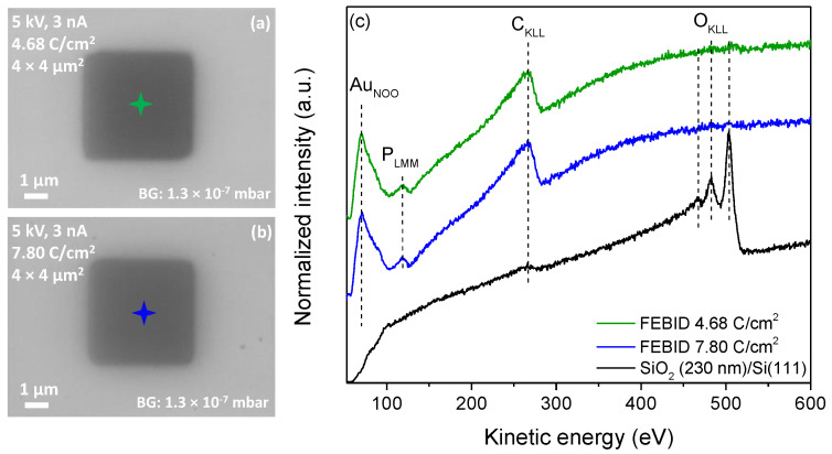
Figure 2.
(a) SEM image of a 4 × 4 µm2 FEBID structure deposited on SiO2 from (CH3)AuP(CH3)3 with an electron dose of 4.68 C/cm2 and (b) with an electron dose of 7.80 C/cm2. In both cases, the electron beam parameters are 5 keV and 3 nA, and (c) AES of the SiO2 substrate prior to deposition (black line) and AES from FEBID structures (green and blue lines). The colored stars in (a,b) indicate the position where the spectra were acquired.

