
Figure 1:
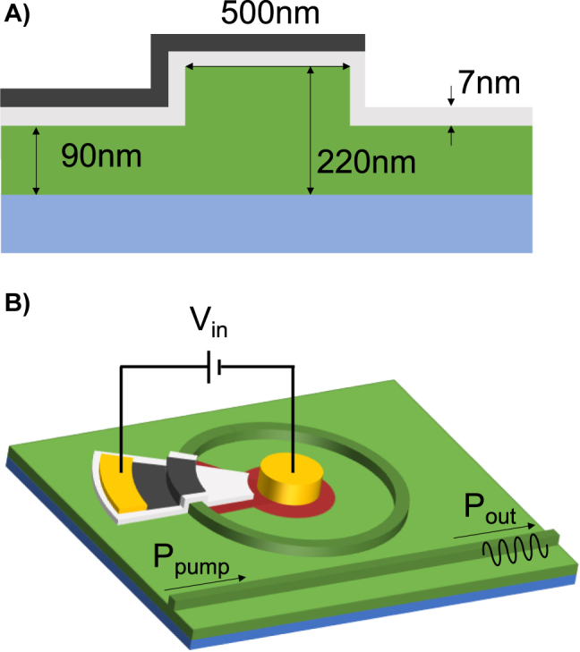
The physical structure of the proposed device. Note the diagram is not to scale for clarity. (A) The cross section where the graphene (black) is over top of the silicon rib waveguide (green) separated by a gate aluminum oxide layer (gray). The waveguide is over silicon dioxide (cyan). (B) The microring resonator with a bus waveguide that carries the input and output power. Voltage bias is applied to metal contacts (gold) and doped silicon (red) to change the Fermi level of the graphene.