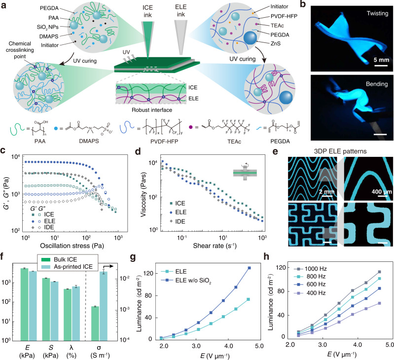
Fig. 2. Ink Design for Direct Ink Writing (DIW).
a Schematic illustration of the multi-material printing process for fabricating an EL device, which consisted of two ion conducting elastomer (ICE) layers and one electroluminescent elastomer (ELE) layer. The addition of SiO2 nanoparticles in the inks leads to physically-crosslinked gels, which are fluidized by the shearing force during ink extrusion and can be recovered to the gel state right after printing. Further UV-initiated polymerization of DMAPS/PEGDA or TEAc/PEGDA leads to the formation of an intact network structure. b Images of the 3DP EL devices under mechanical deformation (i.e., twisting and bending), which are powered with an alternating current. Scale bar: 5 mm. c Shear storage moduli (G') and loss moduli (G'') of the ICE, ELE, and IDE inks as a function of shear stress at 25 ∘C, measured under an oscillatory mode at a frequency of 1 Hz. d Apparent viscosity of the optimized ICE, ELE, and IDE inks as a function of shear rate at 25 ∘C. e Images of the high-fidelity electroluminescent prints of the ELE patterns. f Summary of the physical parameters (i.e., modulus (E), strength (S), elongation at break (λ) and conductivity (σ)) of the ICE samples fabricated from both molding and the 3D printing techniques. g Plotting of the luminance intensity of the 3DP ELE patterns using inks with or without SiO2 NPs against the applied voltage per thickness (E) (thickness of ELE layer was 150 μm, frequency of the applied voltage was 500 Hz). h Plotting of the luminance intensity of the 3DP ELE patterns against the applied voltage per thickness (E) at various frequencies of the applied voltage. Data in f, g, and h are means ± S.D., n = 3 independent samples.

