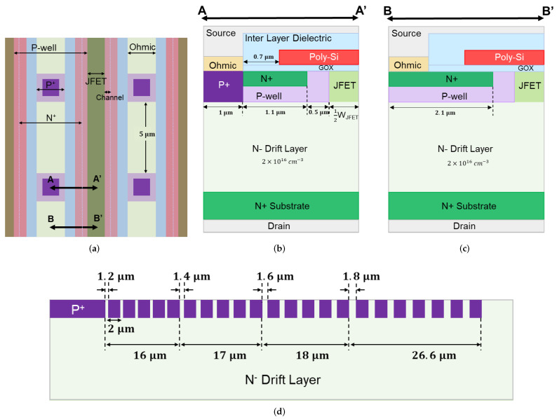
Figure 1.
(a) Layout design of a SiC power MOSFET with located periodically in the center of P-well stripe; (b) A-A′ cross-sectional view showing both and ; (c) B-B′ cross-sectional view showing extended source; (d) cross-sectional view of the edge termination of the fabricated 650 SiC power MOSFETs.

