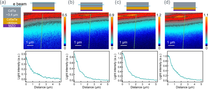
Figure 4.
Mapping carrier transport inside the stressed CdSeTe/CdTe device, with an electron beam fixed in a line scan to excite carriers in different regions, its corresponding transport imaging, and a representative line profile marked in green line (not to scale). (a) Excitation in the CdTe layer; (b) excitation in the CdSeTe intermixture region; (c) excitation in the CdSeTe intermixture region, closer to CdSeTe; and (d) excitation in the CdSeTe layer.

