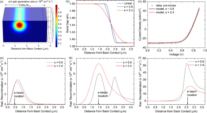
Figure 6.
Device modeling results. (a) 3D rendering of 2D TI simulation showing the e–h pair generation rate at the electron beam location d = 1.4 μm (excitation in MZO and SnO2 not shown); (b) CdSeTe band-gap smoothing variations; (c) simulated J–V curves and comparison with experimental data for a typical device; and (d–f) radiative recombination rate profiles with electron beam excitation at different locations relative to the distance to back-contact.

