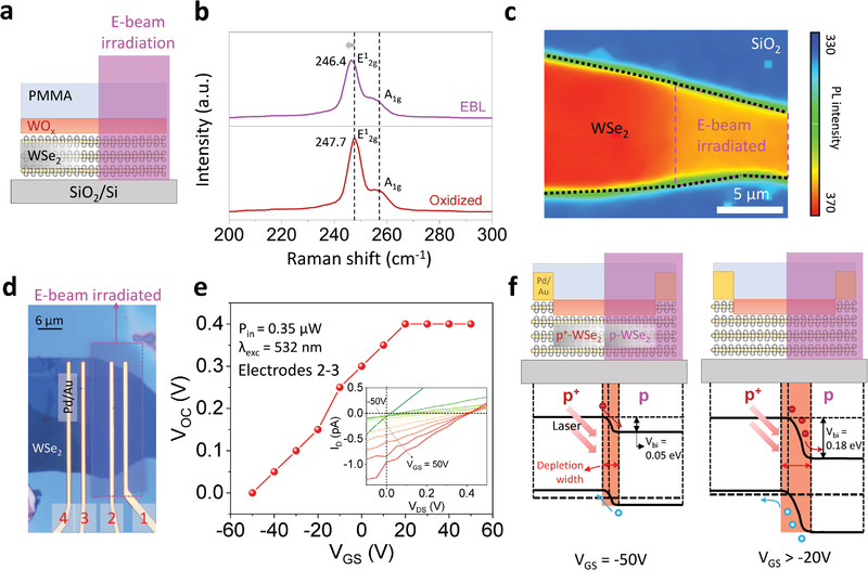
Figure 1.

Oxidized WSe2 with e‐beam irradiation. a) Schematic of oxidized WSe2 sample used for optical measurements to probe the doping effect of e‐beam irradiation. b) Raman spectra of the oxidized WSe2 before and after e‐beam irradiation. c) PL intensity mapping at 760 nm (≈1.64 eV) displays a neutral exciton of e‐beam irradiated and non‐irradiated oxidized WSe2. d) Optical image of seamless junction diode made of oxidized WSe2 patterned by e‐beam irradiation. e) V OC at various V GS measured from the seamless junction diode (measured between electrodes 2 and 3). The inset shows output curves at different V GS under laser illumination with a power of 0.35 µW, wherein the curves indicate the V OC modulation in photovoltaic effect. f) Band alignment of the p+–p WSe2 homojunction at V GS = (−50 and −20) V.
