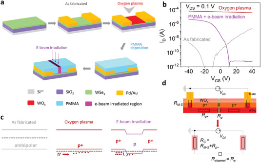
Figure 2.

Electrical analysis of the device according to fabrication steps. a) Schematic of device fabrication, b) transfer curves, and c) band structures of the device at different process steps; as‐fabricated, oxygen plasma treated, and e‐beam irradiated after PMMA passivation. d) Equivalent circuit of the device consisting of three resistances in series (R M−S, R p+, and R p). Here, R C is expressed as the sum of R M−S and R p+, and R channel as R p.
