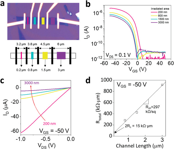
Figure 3.

Contact properties of the p+–p–p+ junction device obtained by TLM measurement. a) Optical micrograph and schematic of the TLM device. b) Transfer curves and c) output curves of devices with several e‐beam irradiated lengths ranging from 200 to 3000 nm with a fixed contact extension length of 1.5 µm. d) R total as a function of channel length to extract R C and R sh by TLM fitting.
