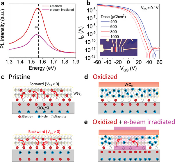
Figure 4.

a) PL spectra of WSe2 after oxidation and e‐beam irradiation showing a red‐shift in neutral exciton. b) Transfer curves of the devices showing strong dependence on e‐beam area dose ranging from 400 to 1000 µC cm–2. The e‐beam irradiated length was fixed at 120 nm for all the tested devices, as shown in the inset. c) Induced hysteresis by interface trap charges at forward and backward bias sweeping for the pristine WSe2 device. Charge states in d) oxidized WSe2 and e) seamless p+–p–p+ junction formed by e‐beam irradiation with forward bias considering the interface trap charges as depicted in (c).
