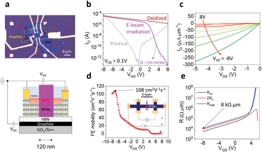
Figure 5.

Graphite back‐gated p+–p–p+ 2D WSe2 FET. a) Optical micrograph and schematic of the device. b) Transfer curves measured at each fabrication step. c) Output curves after e‐beam irradiation showing high saturation current. d) Field‐effect mobility of the device after e‐beam irradiation. e) R ch and 2R C extracted from the four‐probe measurement.
