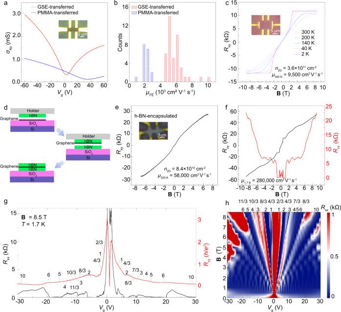
Fig. 3. Electrical properties of transferred graphene.
a Transfer characteristics comparison of two typical Hall-bar devices fabricated with PMMA- and GSE-transferred graphene. Inset: image of graphene Hall-bar device on SiO2/Si. b Histograms of FET mobility of GSE- and PMMA-transferred graphene. The average mobility of 42 GSE-transferred and 18 PMMA-transferred graphene devices are 6000 cm2 V−1 s−1 and 2000 cm2 V−1 s−1, respectively. c The change in Hall resistance as a function of magnetic field of GSE-transferred graphene on SiO2/Si at different temperature. Inset: image of graphene Hall-bar device on SiO2/Si. d The fabrication scheme of h-BN-encapsulated transferred graphene. e The change in Hall resistance as a function of magnetic field (B) of h-BN-encapsulated transferred graphene at 300 K. Inset: image of h-BN encapsulated graphene Hall-bar device. f The variation in Hall resistance (Rxy) (left axis) and longitudinal resistance (Rxx) (right axis) as a function of B at 1.7 K. g Rxx (left axis) and Rxy (right axis) as a function of the back gate (Vg) at 1.7 K and 8.5 T. h 2D contour plot of Rxx as a function of B and Vg. The dash black lines show LLs at filling factors ν = ±2, ±6, and ±10, as well as some new emerging fractional filling factors ν = 2/3, ±4/3, 7/3, ±8/3…, due to the degeneracy lifting of LLs.

