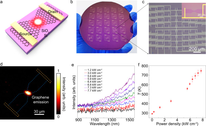
Fig. 4. Integration and radiation properties of wafer-scale graphene thermal emitters.
a A schematic diagram of graphene thermal emitter. b Wafer-scale graphene thermal emitter arrays on GSE-transferred graphene. c Optical microscopy image of 8 × 8 graphene thermal emitters. Inset: single graphene thermal emitter device. d Image of thermal emission at P = 3.0 kW cm−2 captured by IR camera with false-color treatment. The bright spot in the center represents the radiation emitted by graphene. The blue dashed line and yellow dashed line indicate the graphene and metal electrodes, respectively. e Emission spectra issued from a graphene emitter at P = 1.2–7.7 kW cm−2. f Graphene lattice temperatures obtained by the shift in 2D peak’s position. The temperatures varied approximately linearly with power density. Error bars indicate standard deviations of temperatures at different power density.

