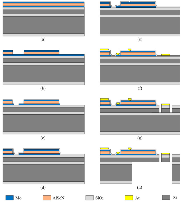
Figure 5.
Fabrication process flow. (a) Deposition of the bottom electrode Mo, the piezoelectric layer AlScN, and the top electrode Mo on LPCVD SiO2; (b) Patterning the top electrode Mo and wet-etching AlScN using 25% TMAH at room temperature; (c) Patterning the bottom electrode Mo; (d) Depositing PECVD SiO2 on the top Mo; (e) Dry-etching PECVD SiO2 by RIE; (f) Sputtering and etching of Ti and Au; (g) Etching the device layer through DRIE; (h) Patterning the handle layer to release the device.

