Figure 1.
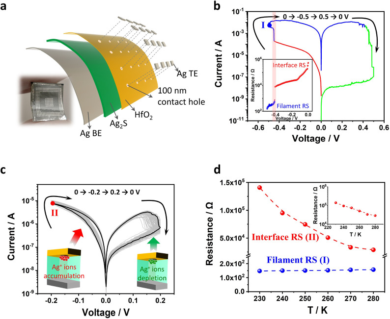
Full-inorganic Ag2S flexible memristor. (a) Schematic illustration of FM structure. The device consists of a silver top electrode (Ag TE), 5 nm thick HfO2 dielectric layer (through which 100 nm contact holes are etched), 100 μm thick Ag2S electrolyte, and silver bottom electrode (Ag BE). The photography in the lower left shows the bended Ag2S FMs. (b) Current (I)–voltage (V) characteristics of FM under 0 V → −0.5 V → 0.5 V → 0 V voltages applied to the Ag TE.23 The inset shows resistance reduction under negative setting bias, where interface RS (setting bias < −0.4 V) is observed before filament formation. Device set by −0.5 V bias is marked by stage I in the curve. (c) I–V characteristics of FM under 0 V → −0.2 V → 0.2 V → 0 V voltages applied to the Ag TE. As schematically illustrated, the device is set by the Ag+ ion accumulation induced SBH reduction and reset by the Ag+ ion depletion induced SBH increase at the top contact interface. Device set by −0.2 V bias is marked by stage II in the curve. (d) Device resistance evolution under temperature variations. Different resistance–temperature dependences indicate filament RS for stage I and interface RS for stage II. The inset shows an exponential relationship between device resistance (at stage II) and temperature.

