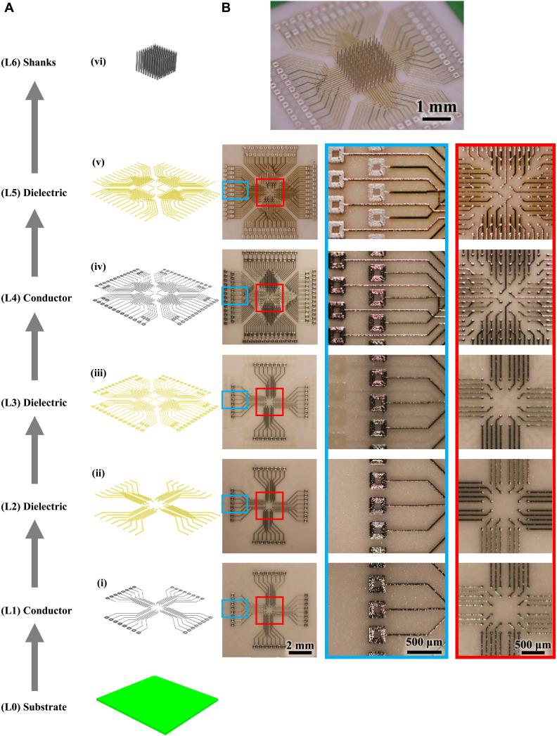
Fig. 3. Electrical routing of the high-density shanks.
Multilayer metal-polymer printing to fabricate a custom board to route signals from high-density MEA. (A) Schematic of the step-by-step process of printing the multilayer board shown via an exploded view and (B) optical images of the printed board. The layers are indicated as (i) to (vi) from bottom-up. (i) Printing of first metal layer on alumina ceramic with pads at both ends of each line. (ii) Polyimide printing to insulate the metal lines except at the pads. (iii) Middle polyimide layer to isolate the layer 4 from layer 1. (iv) Printing of the upper metal layer to create two conductive layers routing the signal out. (v) Polymer insulation printed on the upper metal layer except at the pads on the two ends. Note that the signal routing can be customized by simple changes to the printing program, allowing arbitrary locations and heights for the probes and pads. (vi) Printing of shanks on open pads via the AJ printing process to give a 100-shank probe over an area of 2 mm by 2 mm with printed multilayer wiring/routing.

