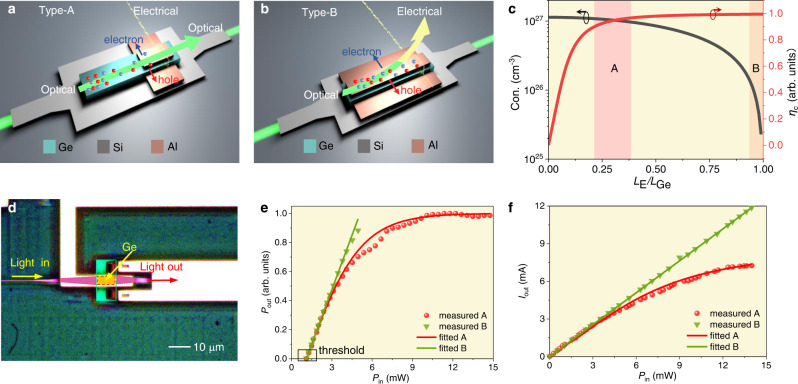
Fig. 2. Theoretical and experimental analysis of the Ge-Si AONU.
a The structure and schematic of the proposed AONU (Type-A). A large number of carriers are accumulated in the non-electrode part of the Ge film, which enhances the nonlinear interaction with light. At the tail end, the carrier movement forms the photocurrent that served as a monitoring signal. The yellow wave ray represents the data flow of the electrical monitoring signals. b The structure of the conventional Ge-Si PDs (Type-B). c The carrier concentration and collection efficiency versus length ratio. Con., concentration. d The false-color image of the AONU. Pink region, Si waveguide. Yellow region, Ge film. Green region, Si slab under Ge film. Red region, metal contacts on Si. The optical signals travel from the Si waveguide into Ge film via evanescent coupling for the desired response. e The measured and fitted Pout-Pin relations. Here, the output optical power is normalized. The actual output optical power of the AONU is between 0 and 1.6 mW under different input optical power, with the optical loss being estimated to be 6.2 dB. The optical loss can be reduced to <3 dB by reducing the optical absorption length or operating at a longer wavelength (with a lower optical intrinsic absorption coefficient). Please see Supplementary Note 5 for more details. f The measured and fitted output photocurrents as a function of input optical power.

