
Figure 2.
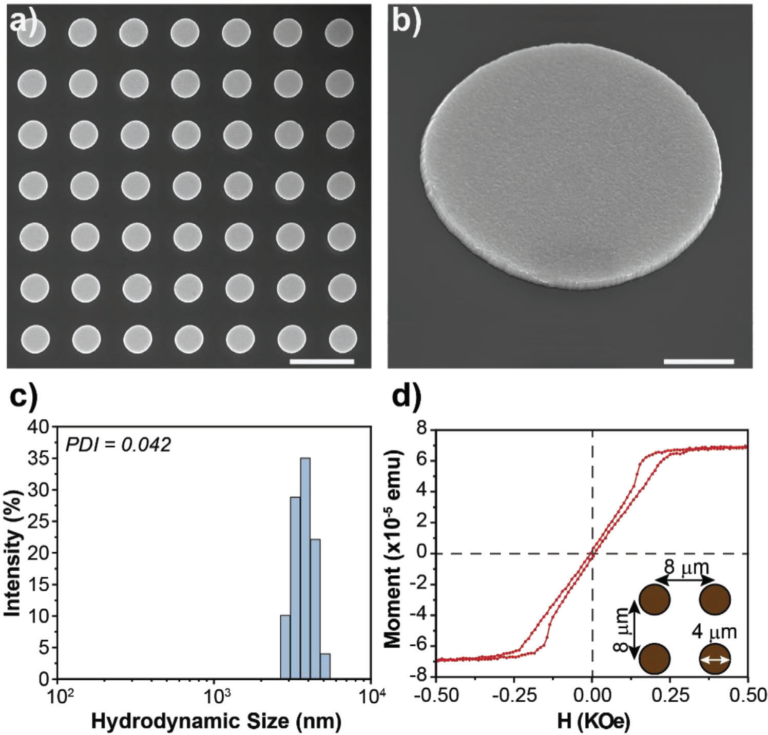
MMDs characterization. a) SEM image of MMDs on the Si wafer. Scale bar = 10 μm, b) SEM image of a tilted single MMD on the Si wafer. Scale bar = 1 μm, c) Hydrodynamic size distribution of MMDs in water after being released from the Si wafer, and d) Hysteresis loop of a square array of MMDs after photoresist liftoff and before release from the Si wafer.