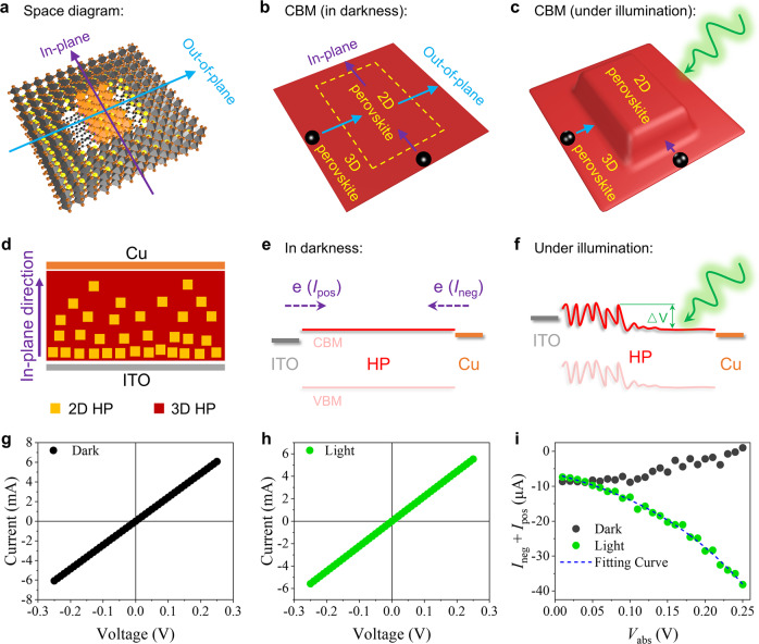
Fig. 6. Theoretical analysis and experimental verification of the PCB effect along the in-plane direction of 2D HPs.
a Space diagram of the 3D/2D/3D HP configuration in typical mixed-dimensional 2D/3D HP films for solar cells. Schematic illustration of the corresponding CBM b in darkness and c under illumination. d Schematic diagram of the ITO/HP/Cu configuration for the in-plane direction measurement; Schematic diagram of the corresponding energy landscapes (e) in darkness and f under illumination. e represents electrons. △V denotes the photoinduced global potential barrier; The I-V characteristics of the vertical ITO/PEA2MA2.67Pb3.67I12/Cu (g) in darkness and h under illumination. i The corresponding (Ineg+Ipos) versus Vabs characteristics in darkness and under one-sun illumination.

