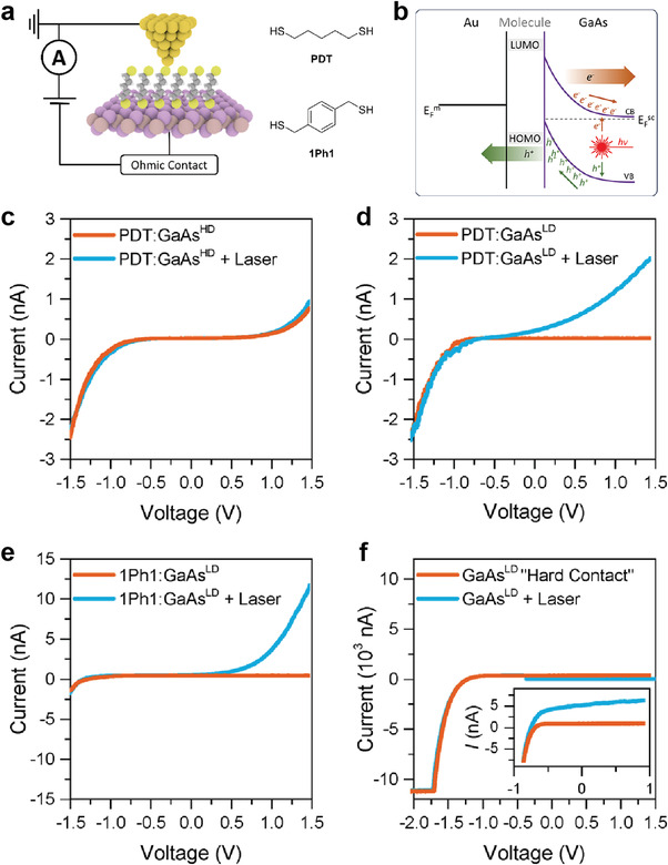
Figure 6.

a) Device schematic and structures of the molecular wires used in this study. b) Schematic band diagram for the illuminated metal‐molecule‐semiconductor junction under reverse bias. Junction I–V characteristics for c) PDT on GaAsHD, d) PDT on GaAsLD, e) 1Ph1 on GaAsLD, and f) “hard contact” between Au and GaAsLD wafers fabricated by crashing the tip several µm into a freshly etched GaAs surface. The inset shows an enlargement of the low‐current area between −1 and 1 V. Reproduced with permission.[ 93 ] Copyright 2017, American Chemical Society.
