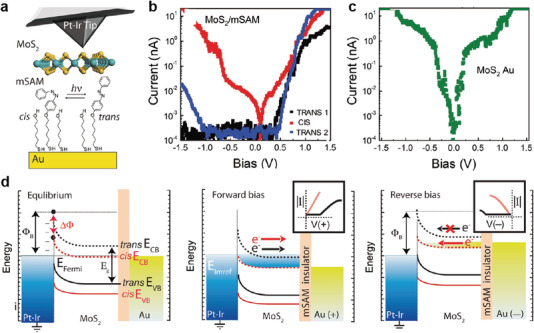
Figure 12.

a) Schematics of the heterostructure measurement. Monolayer and multi‐layers of MoS2 are mechanically exfoliated on top of a mixed‐SAM (mSAM) made of spacer molecules and photoswitchable (black arrow) azobenzene derivatives (1:1) on gold. b) Representative I–V characteristics in semilogarithmic scale for MoS2/mSAM heterostructure before (trans 1) and after UV (cis) and white light exposure (trans 2). c) I–V characteristic for 1L MoS2/Au. d) Schematics of the metal‐semiconductor rectification barrier between the grounded Pt–Ir tip and the MoS2/mSAM Au heterostructure. The transport channel of MoS2/cis‐mSAM is closer to the electrodes’ Fermi levels at equilibrium, and transport readily occurs at any bias. The misaligned transport channel for the MoS2/trans‐mSAM heterostructure at equilibrium requires a larger bias for transport at the corresponding polarities. Reproduced with permission.[ 94 ] Copyright 2015, Wiley‐VCH.
