
Figure 17.
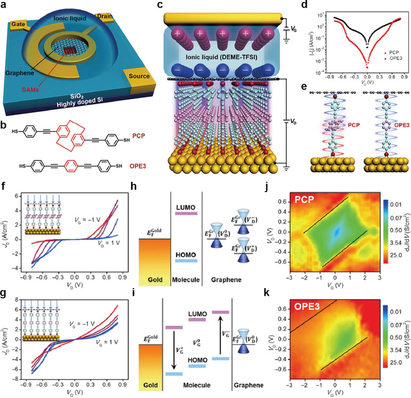
a) Schematic illustration of the overall device structure. b) Chemical structure of the PCP and OPE3 molecules. c) Schematic illustration of the molecular transistor with OPE3 SAMs and ionic liquid (DEME‐TFSI) gating. DEME+ ions are the cations, and TFSI− ions comprise the anions. d) Plots of experimental current density (J D) versus bias voltage (V D) for PCP and OPE3. e) Schematic illustration of the PCP and OPE3 junctions. J D versus V D characteristics for f) PCP and g) OPE3 with gating from −1 to 1 V with step of 0.5 V. h) Schematic band diagram of the device under varying V D at graphene electrode. i) Schematic band diagram of the device under varying V G. 2D visualization of dJ/dV plotted with respect to V G and V D for j) PCP and k) OPT3. Black lines in (j) and (k) are auxiliary markers of corresponding conductance diamond edge. Reproduced with permission.[ 208 ] Copyright 2018, American Association for the Advancement of Science.