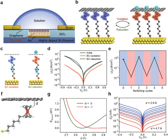
Figure 18.

a) Schematic illustration of the device structure of Au/Fc‐SAM/SLG junction with a liquid drop on top of the chip. b) Schematic illustration of the Au/Fc‐SAM/SLG junction with oxidation and reduction treatments. c) Schematic illustration of the EC‐oxidation and EC‐reduction with controlled electron transfer processes. d) J D–V D curves for the junction in initial state, treated by EC‐oxidation and re‐treated by EC‐reduction. The error bars represent the log‐standard deviation. e) Corresponding |J D| at V D = −0.5 V for the junction sequentially treated by EC‐oxidation (red) and reduction (green). f) Schematic representation of the Fc‐graphene contact, where d is the contact separation. g) Ground state energy versus d for different number of electrons N on the molecule: N = 0 (neutral) and N = −1 (oxidized). h) I–V characteristics for contact distances of d changed from 2.9 to 4.7 Å with step of 0.2 Å. Reproduced with permission.[ 212 ] Copyright 2022, Elsevier Inc.
