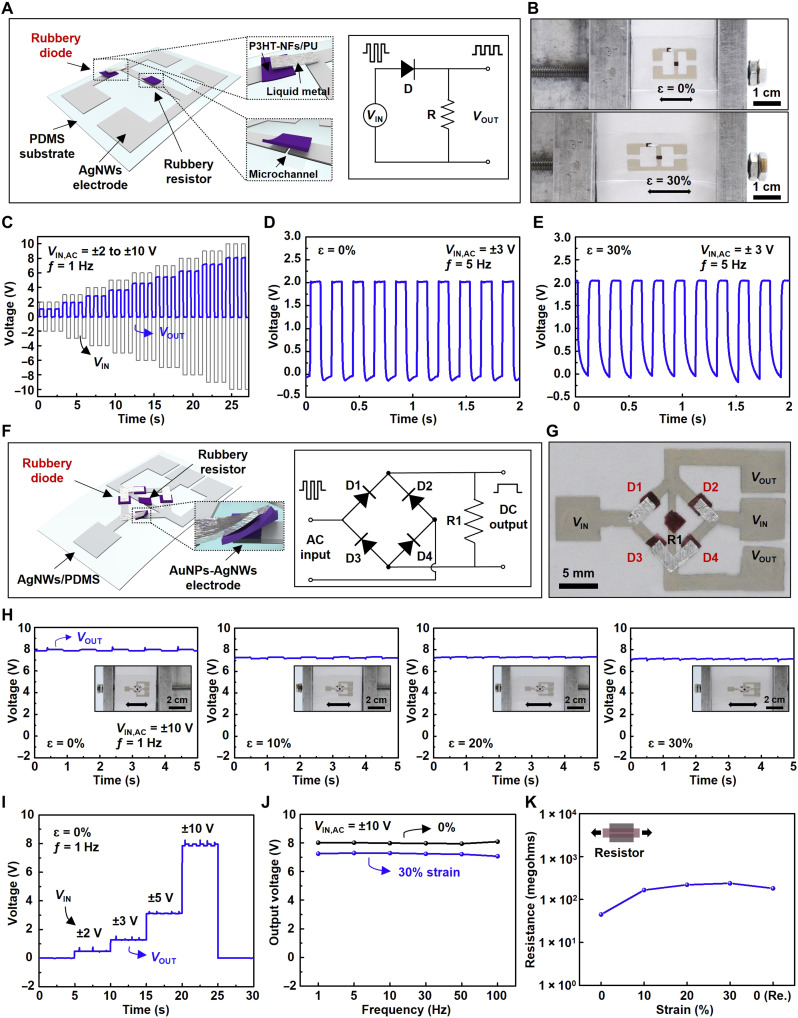
Fig. 2. Fully rubbery rectifiers.
(A) Schematic illustration of the half-wave rectifier and circuit diagram. (B) Optical images of the half-wave rectifier under the mechanical strain of 0 and 30%. (C) Rectified output voltages with different input voltages from ±2 to ±10 V (1 Hz). (D and E) Output voltage with VIN,AC = ±3 V, 5 Hz under the mechanical strain of 0% (D) and 30% (E). (F) Schematic illustration of the rubbery full-wave bridge rectifier and circuit diagram. (G) An optical image of the full-wave bridge rectifier. (H) Output voltages with ±10 V (1 Hz) under the mechanical strain of 0, 10, 20, and 30%. (I) Output voltages with different input voltages of ±2, ±3, ±5, and ±10 V (1 Hz). (J) Frequency characteristics for the full bridge rectifier with ±10 V input voltage under the mechanical strain of 0 and 30%. (K) Resistance of the rubbery resistor under the mechanical strain of 0, 10, 20, 30, and 0% (released) perpendicular to the channel length.

