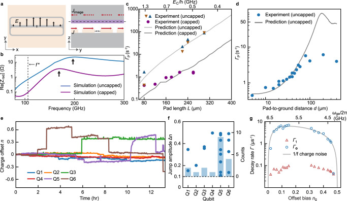
Fig. 3. Effect of circuit geometry on parity switching, charge offset stability, and coherence.
a Top view of the electric field (E, arrows) of the fundamental radiation mode formed by the floating transmon structure (left). Mode current (J, solid arrows) and its image (Jimage, dashed arrows) on the two sides of the aluminium cap indicated by the dashed line (right). b Real part of the simulated input impedance Zrad of a typical qubit (L = 260 μm, W = 35 μm) with and without a cap. The arrows indicate the peaks corresponding to the fundamental mode. The dashed line indicates the superconducting gap frequency at 105 GHz. c Measured parity switching rates for capped (dots) and uncapped (triangles) qubits with varying pad size plotted as a function of the pad length. In the uncapped case, the pad width is also varying, but the effect is much smaller. The solid lines indicate finite-element simulation predictions. The top axis indicates the charging energy EC that corresponds to the different pad lengths in the capped case. d Measured (dots) and simulated (line) parity switching rate of qubits with varying pad-to-ground distance d. e Offset charge drift for six qubits on a single chip (Fig. 1a) with the same pad size but varying pad-to-ground distance (d = 5 − 30 μm), simultaneously monitored over a 13-h period. f Amplitudes (dots, left axis) and total counts (bars, right axis) of all offset charge jumps (∣Δq∣) >0.1e identified in the data in c and the extended data (Supplementary Material) during a total of 40 h of monitoring. g Measured relaxation (Γ1) and pure-dephasing (Γϕ) rates of Q1 as a function of ng sampled over half a period. The top axis indicates the corresponding qubit frequency. The solid line is fit to the 1/f charge noise model. It is difficult to characterize the qubit around ng = 0.25 because of the stronger sensitivity to charge noise around this bias and because of its adjacency to the resonator at 5.55 GHz.

